Fabrication of Polymeric Waveguide Bragg grating filter using a replication process
高分子波導布拉格光柵濾波器之研製
Wistek
Lab.
Lee Kun-Yi 1, Lin Yen-Juei1, Lin Kuen-Cherng1, Chuang Wei-Ching2, and Lee Wei-Yu1
Abstract
In this paper, we fabricate a polymeric waveguide Bragg grating filter using a replication process. The grating structure on a polymer is fabricated using holographic interferometry and micro-molding processes. The polymeric waveguide Bragg grating filters are produced by a two-step molding process where the master mold is first formed on a negative tone photoresist and subsequently transferred to a PDMS mold; following this step, the PDMS silicon rubber mold was used as a stamp to transfer the pattern of the polymeric waveguide Bragg grating filters onto a UV cure epoxy. Initial results show good pattern transfer in physical shape. At the Bragg wavelength, a transmission dip of -15.5 dB relative to the –3dB background insertion loss and a 3-dB-transmission bandwidth of ∼6nm were obtained from the device.
摘要
本論文運用一種複製流程研製高分子波導布拉格光柵濾波器。高分子光柵結構是以全像干涉及微成形制程製作。高分子波導布拉格光柵濾波器經由二階段鑄模制程,首先,具光柵圖案之主模仁成型於一負光阻,其次,藉由該負光阻模仁再將光柵圖案轉移到一個聚二甲基矽氧烷(PDMS)薄膜模仁上;而後,再以聚二甲基矽氧烷(PDMS)模子把光柵圖案,轉移到經紫外線固化成型的環氧樹脂上,進而完成元件的製造。初步實驗結果證實,經由本論文之制程可得到高解析之光柵結構,而且在布拉格波長有-15.5 dB之傳輸降幅及6nm之3-dB傳輸頻寬。
Key Words: polymeric waveguide, Bragg grating filter, holographic interferometry, micro-molding process
關鍵字:高分子波導、布拉格光柵濾波器、全像干涉、微成形制程
中圖分類號:TN814+.6、TN713+.1、O436.1
1. Introduction
Optical grating filters in guided-wave optics have been extensively investigated [1-2], because they are essential for applications in wavelength division multiplexing systems. For optical filter applications, high-resolution and high aspect ratio grating fabrication is important because they impact the filtering characteristics and compact size of the devices.
Polymeric optical devices are widely used in guided-wave optics owing to their low cost and simple fabrication process. Realization of Bragg gratings in polymer waveguides has attracted much attention in optical communications and optical sensing systems. Typical techniques for patterning gratings on polymer films include holographic lithography, electron-beam lithography, laser beam direct writing, and phase mask lithography. However, few researchers have focused on fabricating surface-relief grating on channel waveguides.
We have recently demonstrated a process to rapidly produce submicron range gratings by using both micro-molding and holographic interference techniques. A large aspect ratio of 0.7:1 between the depth and the period on the grating pattern could be obtained, and consistent reproduction of the grating on a UV polymer could be achieved with this process [3]. In this paper, we demonstrate a method to inscribe surface-relief gratings on polymer channel waveguides without any physical etching process.
There are a number of simple methods to fabricate polymer waveguides that include techniques involving hot embossing, UV-embossing, and micro-transfer molding method are also becoming more popular due to their simple fabrication procedure. However, these methods have problems to overcome; such as residual material problems and limited substrate and core materials available [4-5]. We have recently developed a soft lithography method to replicate polymer waveguides [6]. In this method, the waveguides are produced by a two-step molding process where a master mold is first formed on a negative tone photoresist and subsequently transferred to a PDMS mold. The silicone rubber mold is then used as a stamp to transfer the final waveguide pattern onto a UV curing epoxy. High aspect ratio (depth/ width) and vertical waveguide sidewalls could be obtained by this method.
In this paper, we will describe a technique that combines the holographic interferometry, soft lithography, and a simple replication processes to create a high resolution and high aspect ratio grating structure on a polymer waveguide. In order to reduce the residual stress caused by different thermal expansion coefficients in the core and cladding material, similar polymer materials with slightly different index are used for the core and cladding layers. The material has a refractive index between 1.52~1.56 (OG146=1.5201, and OG154=1.5668) at wavelength 1550nm, which is close to the refractive index of optical fiber (about 1.46-1.50).
2. Grating Fabrication
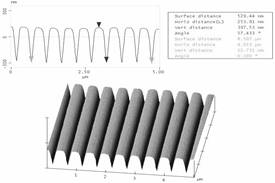
Rapid prototyping of grating structures on a polymer substrate involving a three-step process was performed first. A grating pattern is holographically exposed using a two-beam interference pattern on a positive photoresist film (Ultra 123 made by MicroChem Corp., MA., refractive index = 1.618). This produces a master that can be subsequently used to produce a polydimethylsiloxane (PDMS) mold. This silicone rubber mold then is used as a stamp to transfer the gratings pattern onto a UV cure epoxy polymer. The details of the process involved for the grating fabrication was described in our previous reports [3]. Based on our results, we found that the grating period and the corresponding depth of the grating pattern can be accurately controlled down to less than 1% error. We also found that a high aspect ratio of almost 0.7:1 between the depth and the period of the grating structure could be obtained. Figure 1 shows the AFM and SEM results of OG146 with a grating period of 503nm and a grating depth of 397nm, which was fabricated by the above process. The UV polymer with grating was cut down to 1cm x 5cm, and the dimensions of the gratings on polymer were 0.5cm long and 1mm wide.
(a)
 (b)
(b)
Fig.1. AFM and SEM micrographs of gratings on UV polymer (a) AFM (b) SEM (503 nm grating period and 397 nm grating depth)
3. Fabrication of the polymeric wavelength filter
In order to fabricate polymer wavelength filters, a 700μm thick glass substrate was first cut into a 5cm x 1cm rectangle. After substrate cleaning, the UV polymer was put on the glass, and it was coated with a 6.0 μm thick negative photoresist (SU-8) spun on at 1000rpm for 17 seconds. Samples were exposed through the PET (Polyethylene Terephthalate)-based masks using a UV mask aligner (AB-Manufacturing, CA) for 90 seconds, followed by developing in a SU-8 developer (MicroChem) for 45 seconds, and negative waveguide pattern with gratings on the bottom were obtained. The process flow is shown in Fig. 2(a) and (b). The waveguide dimension is about 8.7μm x 6.0 μm, and the length is about 5cm. The patterned resist was used as a mother mold to transfer the pattern onto a polydimethylsiloxane (PDMS) thin film using typical micro-molding technique(e.g. stamping). The diluted PDMS was uniformly coated on the patterned photoresist. After baking at 90°C for 1 hr, the PDMS was cured and could be easily peeled off from the photoresist (Fig. 2(c)-(e)). The waveguide with the gratings pattern was transferred onto a UV polymer (OG146) from the PDMS mold using a UV replication process(Fig. 2(f)-(h)). A spacer with a thickness of 400μm was placed between the mold and a thin Pyrex glass slide. After injection of the precure UV polymer (OG146), the epoxy was then cured under a broadband UV light operating in a wavelength range of 300-400nm. After the polymer was fully cured, the polymer was easily peeled off from the mold. After separating from the PDMS mold, a hardened epoxy with gratings forms the cladding layer of the polymer waveguide filter.
To form the waveguide core, a similar UV epoxy (mixed OG) is injected into the groove. Instead of spin coating technique, which could create a thick unguided layer outside the core region that would results in some coupling loss during the input of the optical fiber to the filter, another method was also proposed (Fig. 2(i)-(j)). A thin layer of a polydimethylsiloxane (PDMS) polymer was spun onto a glass slide that is then placed over the epoxy groove, forming a rectangular tunnel. In order to inject the high viscosity epoxy of OG154 into the rectangular channel, we diluted the OG154 with another UV epoxy OG169 (the mixing ratio is 1:1) to reduce the viscosity of the OG154. After the curing process, the refractive index of the mixed epoxy is about 1.550 at 1550nm. Then, a drop of the mixed UV epoxy was injected into the channel from one of the open ends. After exposing with UV light, the epoxy end of the tunnel was sealed. Next, the sample was inserted into the liquid epoxy with the open-end face down. This process was performed in a vacuum chamber (Fig. 2(i)). When the pressure in the chamber reached 10-4 Torr, air was introduced into the chamber to force the liquid epoxy into the tunnel. The epoxy in the tunnel was cured by exposing the UV light for 1-2 minutes. After the cover glass was removed, the PDMS layer was peeled off from the sample. To prevent the optical loss due to either surface scattering losses or the outright absence of a guided mode for the asymmetric waveguide structure, the upper cladding layer was used. The same UV epoxy (OG146) was deposited using the fabricating procedure described in the previous section (Fig. 2(k)-(n)). A spacer with thickness of 410μm was placed between the sample and a thin Pyrex glass slide. After injecting the precure UV polymer (OG146) into the opening between the mold and the glass slide, UV light was used to crosslink the polymer. The sample were diced and the end-faces were then polished, such that the final polymeric wavelength filter has dimensions of 4cm in length, 1cm in width and about 410μm in thickness (Fig. 2(n)).
The waveguide properties including the mode pattern and the effective index were simulated using the beam propagation method (BPM_CAD, Opti-Wave Inc., Canada). The effective index of the waveguide is 1.5447 from the simulation. The Bragg wavelength is 1553.9 nm as calculated from the Bragg reflection condition. The transmission of the optical filter was also calculated by using coupled mode theory[7]. The calculated transmission minimum of the optical filter is -19.5dB. The spectral characteristics of the optical filter were measured using an optical spectrum analyzer (Q8384 Optical Spectrum Analyzer, Advantest Inc., Japan). Again, an amplified spontaneous emission (ASE) light source with a wavelength range from 1530 to 1560 nm was used as the wide band light source. An alignment He-Ne laser source, as the auxiliary source, was combined with the wide band source using a 2×1 optical fiber coupler. The optical filter was set on a micro-positioner, and two single mode fibers were used as the input and output fibers. The input light source was polarized in the TE direction as was the mode field measurement system. The output fiber, then, was connected to the optical spectrum analyzer to characterize the filter performance. The measured result is shown in Fig.3. At the Bragg wavelength, a transmission dip of –18.5 dB was obtained, and the 3-dB-transmission bandwidth was about 8nm. The result is consistent with the calculation of the coupled mode theory. The Bragg wavelength λB is given as λB=2NeffΛ, where Neff, can be calculated using the beam propagation method, is the effective index of the waveguide grating and Λ is the period of grating. The measured Bragg wavelength is 1554.02 nm, which is off by 0.12nm from the theoretical prediction. When the core refractive index ranges from 1.549 to 1.551 for the ratio of OG154 ranging from 45% to 55%, the calculated Bragg wavelength by the beam propagation method varies from 1552.9 to 1554.8 nm.
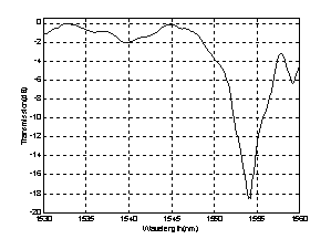
Fig.3.Transmission spectrum of the polymeric wavelength filter with 0.5cm-long grating length
4. Conclusion
In conclusion, we have successfully created a process to rapidly produce submicron range gratings on polymer waveguides by using holographic interference techniques, soft Lithography, and micro molding. A large aspect ratio grating pattern could be obtained with consistent reproduction of the grating on a UV polymer waveguide could be produced. The grating period and depth on the polymer waveguides exhibited only a small difference from the original designed grating pattern. This process shows great potential for mass production of any period of grating structure on waveguide, and could be used to successfully fabricate coupled polymeric waveguide filters.
References
[1] Y. Shibata, S. Oku, Y. Kondo, and T. Tamamura, “Effect of sidelobe on demultiplexing characteristics of a grating-folded directional coupler demultiplexer,” IEEE Photonics Technol. Lett., vol.8, pp.87-89, 1996.
[2] A.W. Ang, G.T. Reed, A. Vonsovici, A.G.R. Evans, P.R. Routley, and M.R. Josey, “Effect of grating heights on highly efficient unibond SOI waveguide grating couplers,” IEEE Photonics Technol. Lett., vol.12, pp.59-61, 2000.
[3] W.C. Chuang, C.T. Ho, and W.C. Wang, “Fabrication of a high resolution periodical structure using a replication process” Opt. Express, vol.13, pp.6685-6692, 2005.
[4] K. E. Paul, T. L. Breen, J. Aizenberg, and G. M. Whitesides, “Maskless Photolithography: embossed photoresist as its own optical element,” Appl. Phys. Lett., vol.73, pp.2893-2895, 1998.
[5] X.-M. Zhao, S. P-Smith, S. J. Waldman, G. M. Whitesides, and M. Prentiss, “Demonstration of waveguide couplers fabricated using microtransfer molding,“ Appl. Phys. Lett., vol.71, pp.1017-1019, 1997.
[6] W.C. Chuang, C.T. Ho, and W. C. Chang, “Fabrication of polymer waveguides by a replication method,” Applied Optics, vol.45, pp.8304-8307, 2006.
[7] A. Yarin, Introduction to Optical Electronics, 3rd edition, (H. Rinehart & Winston, New York, 1984.
.
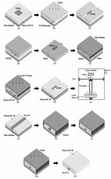
Fig.2. Fabrication process of buried gratings in polymeric waveguide filter structures, a) UV polymer with gratings was deposited on the glass, b) UV light exposure of photoresist, c) photoresist mold, d) PDMS is poured into the photoresist mold, e)PDMS mold, f) A spacer with a thickness of 400μm is positioned, g) OG146 precure epoxy is injected into the space, h) hardened epoxy forms the cladding layer of polymeric waveguide filter, i) forming a rectangular channel, j) Mixed OG epoxy is injected into thechannel, k) The epoxy in the channel was then cured by exposing with UV light, and the cover glass and the PDMS layer are removed from the sample, l) A spacer with a thickness of 400μm was positioned, m) OG146 epoxy is injected into the channel, n)final polymeric waveguide filter.